Bga Ceramic Ball Technique

7 Bottles Of 12 5k Soldering Ball Lead Solder Ball Set For Bga Reballing Stencil
Bga Surface Mount Technology Assembly And Some Tips To Optimize The Process Pcbcart

Solder Ball Issues Of Bga Components And Their Remedies
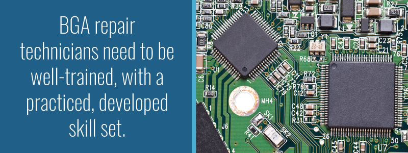
Bga Reballing Training Precision Pcb Services
Types Of Bga Packages And Reballing Each Of Them
A Define Bga Components And Bga Soldering Process
For more information on bga reballing services follow the link below.
Bga ceramic ball technique. Cbga ceramic bg ceramic ball grid array package drawings bg filter packages by entering lead count or product description into the search box below. Ceramic ball grid array package drawings bg view more csp bga chip scale bc ca chip scale package ball grid array package drawings bc ca view more. The bga is descended from the pin grid array pga which is a package with one face covered or partly covered with pins in a grid pattern which in operation conduct electrical signals between the integrated circuit and the printed circuit board pcb on which it is placed. Package outline material information.
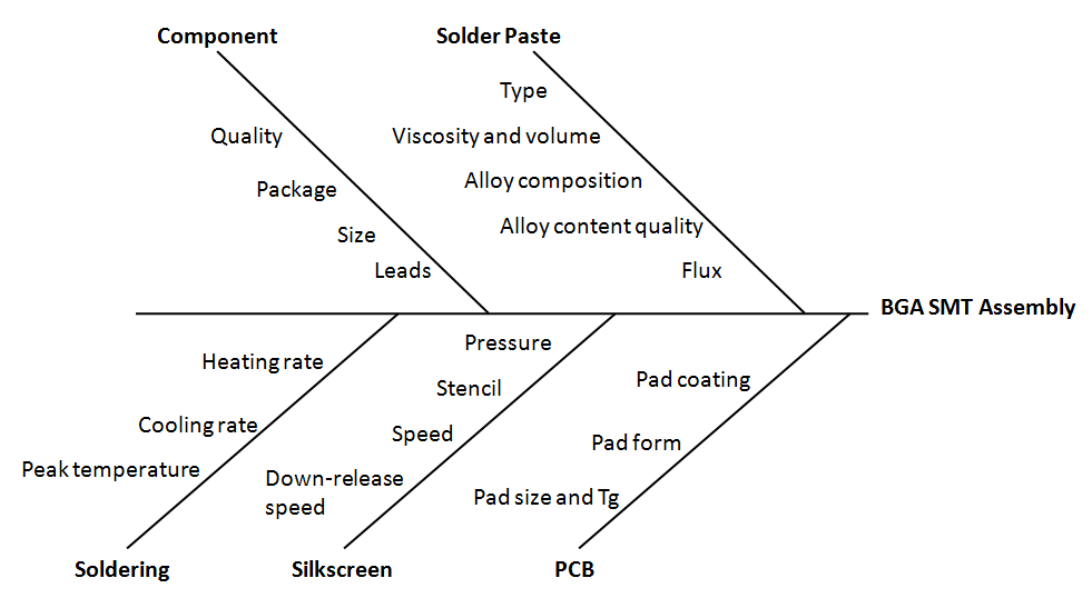
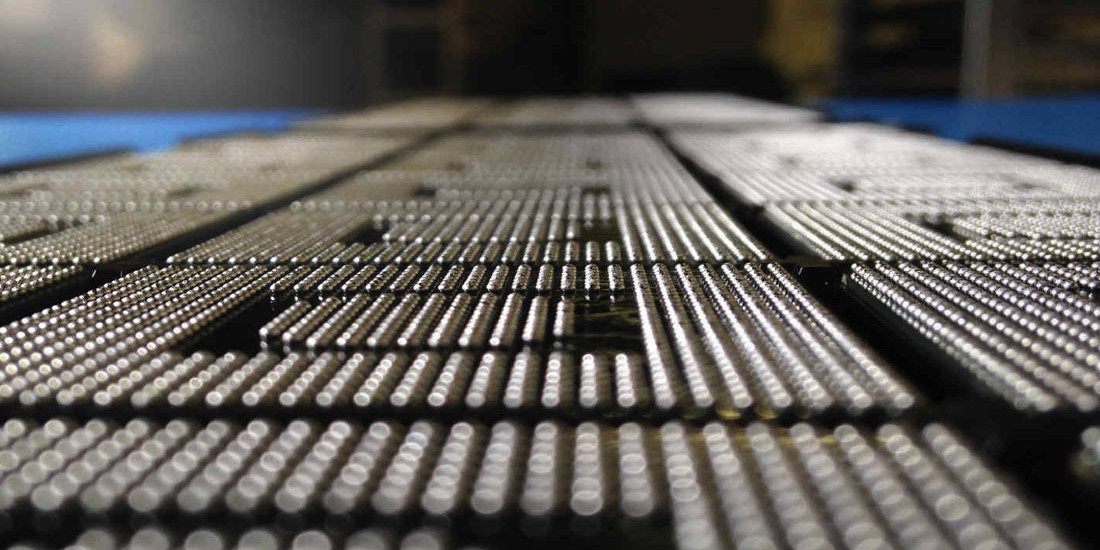
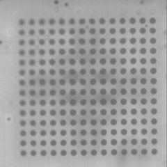
More at wikipedia bga features. In a bga the pins are replaced by pads on the bottom of the package each initially with a tiny solder ball stuck to it. Bga ball grid array a surface bonding encapsulation technique used in integrated circuits. Compared with other packaging technologies bga can accommodate more pins.
In addition to this rather than having the more traditional wire pins for the connections pads with balls of solder are used instead. Advantages are high density low thermal impedance and low inductance pin. The pins of the bga package are arranged in a grid pattern and this gives rise to the name.

Bga Rework Stand Bracket 55 14 5cm Table Accessories Accessories Diy Clamps

5pcs 6pcs Pure Copper 900m T Soldering Iron Tip Lead Free Solder Tips Welding Head Bga Soldering Tools Discount 10 In 2020 Soldering Iron Soldering Tools Welding Tips

80w 220v Eu Plug Electric Soldering Iron Welding Tool Hand Solder Wire Tweezers Lcd Digital Ceramics Constant Temperatur Soldering Iron Welding Tools Soldering

A Top View Of A Bga Pcb Assembly After Cutting And Before Bonding The Download Scientific Diagram

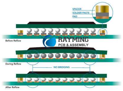
How To Solder Bga On Pcb Board Eeweb
Bga Reballing Services
Common Bga Rework Mistakes And How To Avoid Them

Pdf Ball Grid Array Bga Solder Joint Intermittency Detection Sj Bist

Simple Bga Reballing 9 Steps Instructables
Ball Grid Array Wikiwand

Feorlo 5pcs Lot Wsd81 Soldering Station Stainless Steel Sleeve Wsp80 Solder Iron Handle Weller Feorlo 5pcs Wsd81 Sol Iron Handles Soldering Ceramic Heater
Defect Features Detected By Acoustic Emission For Flip Chip Cga Fcbga Pbga Fpbga Packages And Assemblies

Pdf Development Of A New Improved High Performance Flip Chip Bga Package